Showing posts with label PLD. Show all posts

Friday, October 11, 2013

Gameboy MBC - Which to choose?

Just a quick overview for unfamiliar readers before we get into the thick of it.

The Nintendo Gameboy uses a Memory Bank Controller inside of official cartridges for switching between banks of memory and ultimately expanding the addressable memory. The MBC will switch between banks of both ROM and RAM so that the programmer may code larger games and backup more data in save files.

There are four main MBC's numbered 1 through 5 and excluding 4. The reason I am writing this is because each following revision did not simply add more addressable memory. Each one has unique capabilities built in as well as expanding the addressable memory. in general the MBC's function by waiting for specific data bits to be written to yet more specific memory locations. Once the data in question is written to the specific memory location, the MBC switches the active bank of ROM and RAM to accommodate more code.
I will summarize each MBC as well as quote some information from datasheets.

MBC1


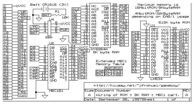
Is the first in the series of controllers which did only expand the addressable memory. Since the gameboy has 16 address pins and 8 data pins running through to the cartridge, the gameboy may without an MBC address only read from and write to a maximum of 256Kbits or 32Kbytes which is incredibly small considering Mario Land has 12 massive levels with multiple means of gameplay including the platformer and shooter, in both an airplane and submarine. Some of these levels even have secondary underworlds where Mario drops to an extra map off screen to collect secret coins or other items.

In any case, the MBC1 has two different modes to choose from. There is the 16Mbit ROM/8KByte RAM and 4Mbit ROM/32KByte RAM. 

Note: RAM is an external IC which needs to be connected to a battery while disconnected from gameboy power to retain data.

MBC2

Similarly to the MBC1, the MBC2 maps extra banks of memory with specific memory writes; however, it may only map up to 2Mbits or 256Kbytes of ROM. Why a decrease? Well the magical thing about the MBC2 is that it contains 512 x 4 bits of SRAM built into the IC itself. This saves a lot of room on your cartridge board granted you are designing one.

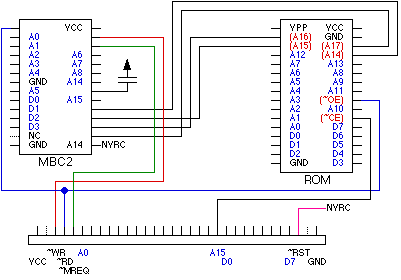
The MBC2 can save money on RAM and space on your board if you are programming a small game that requires little ROM and RAM. Referring to the MBC1 above, if you wanted to offer a saving feature, you would need to source a RAM IC as well and route all of the Address, data and control pins to another location on the board.

MBC3

The MBC3 may again address up to 16Mbits of memory, but has a major feature built like the MBC2 has RAM. The MBC3 has an RTC or Real Time Clock built in. The RTC while still needing battery power when disconnected, offers a real-time count so that games such as pokemon may tell whether it is night or day, or when an hour in real life has passed for example.

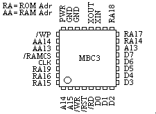
Some games use the MBC3 without utilizing the RTC, but games that do include Pokemon of Generation 2 and Harvest Moon.

MBC5

Lastly, the MBC5 is the final Memory Bank Controller from Nintendo. This particular MBC does not come with internal RAM or an RTC. It simply maps huge amounts of memory. It may map up to 64Mbits of ROM and up to 1Mbit of RAM but not both. There are different configurations to choose from; these are just the maximums.

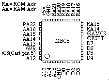
This MBC which I find in nearly every Gameboy Color cartridge regardless of ROM size is guaranteed to work with the GBC's double speed mode. The others seem to work just fine too though, considering any GB game will run on your GBC.

For more information on how to use the MBC's with software, please refer to "Cartridge Types" in this document:
http://www.devrs.com/gb/files/gbspec.txt

MBC CPLD Clones & Reproductions

Aside from the Official Nintendo MBC's, people have had major success in recreating them using CPLD's. Both Homebrew developers and Chinese pirating companies that is.

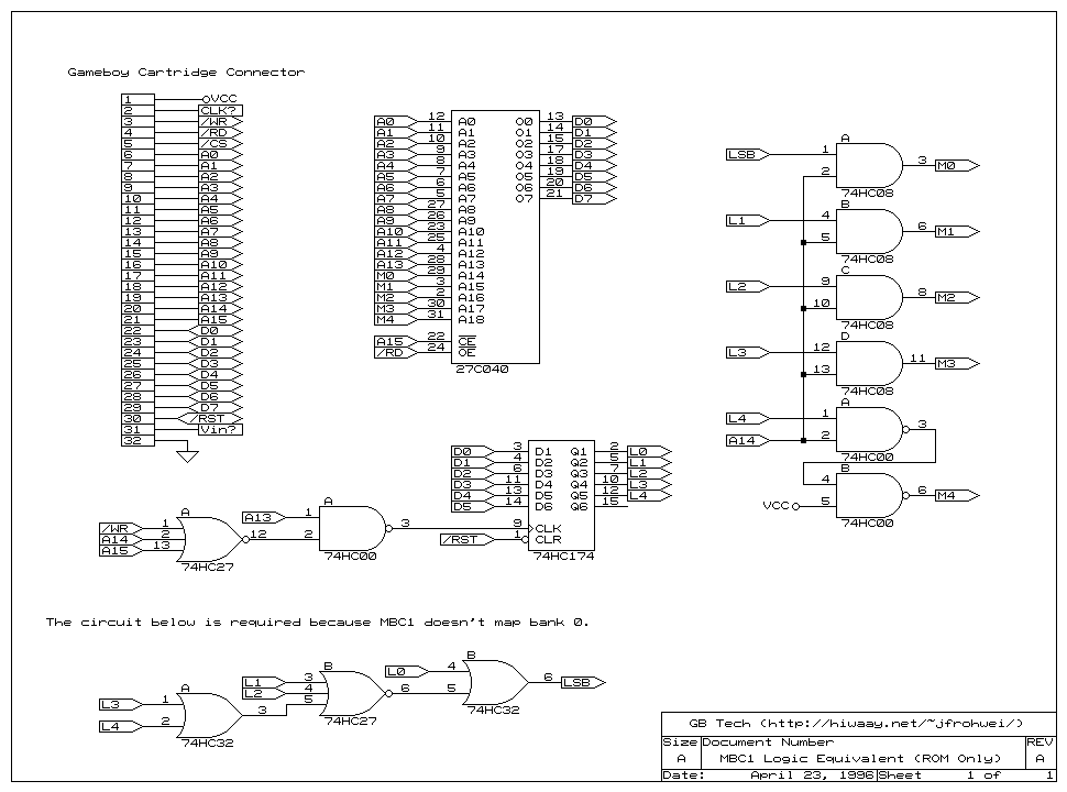
Since the MBC2 and MBC3 contain separate ICs, recreating them is much too difficult for a single person. MBC1 and MBC5 on the other hand can and have been redesigned by using CPLD's. They way they work as mentioned above is that they look for specific data bytes to be written to specific address locations. This Logic can be entirely drawn out using logic gates, which in turn can be programmed onto the CPLD.

MBC1 - CPLD

The MBC1 being the most simple, can be drawn using as little as 11 gates! (granted you do not need RAM)


MBC5 - CPLD

The MBC5 is much more complex of course, but it has also been cloned successfully by at least two separate people using two different CPLD's. One person used the XC9536 and the other person used the XC9572.

XC9536
http://chipmusic.org/forums/topic/2988/mbc5-clone-in-cpld/
and XC9572
http://home1.stofanet.dk/hvaba/gameboy/mbc5cpld/cpldcart.html

Depending on the number of inputs and outputs, more complex logic ought to be designed using PLD's or CPLD's. Not only can you save money on IC's, but space on your circuit boards. More often than not, a logic IC will take up space on your board and have a handful of unused pins and gates which is wasteful and lazy.

As always, thanks for reading! I hope I opened someone's eyes to new and old hardware.
Cheers

Tuesday, September 10, 2013

GameGear CPLD Cartridge

After researching PLD for my Atari dev cart, I remembered a time when I was trying to figure out a Gamegear flash cartridge. It is simple enough, but I had little luck because I was still very unlearned at the time when it came to Addressing bits.

Anyhow, I came across a Caesar's Palace Cartridge by Majesco which utilizes a CPLD! At the time I figured that I would never see one again, nor would I care at all if I were to. Now I care very much because they are pretty damn incredible devices!

The pictured CPLD is by Xilinx and now that I think about it, I really should locate it once more and dump the program on the CPLD. I dumped the game ROM, but it was exactly bit for bit the same as one I ... erm ... 'found' online.

Image Hosted by ImageShack.us Image Hosted by ImageShack.us Image Hosted by ImageShack.us

below is some pictuyres I took when I was trying to make that flash cart. I really wanted to play the Translated Phantasy Star on actual hardware, but I never got to before dropping the project.

Image Hosted by ImageShack.us

My drawing is flawed in that the highest address pins are connected to VCC and I programmed the ROM at the lowest bank which would place it at a point where the highest Address pins would all be low. Haha, silly me. had I simply filled in the extra ROM space with the ROm over and over again, it would have worked. I'll try again in the near future, no worries.

Below are more pictures of the bare board. Good times. lol
See how I ruined a few pins by pulling the pads up? That was a long time ago and I am proud to say that I can do much better.

Image Hosted by ImageShack.us


Image Hosted by ImageShack.us

Even though the game gear is a terrible handheld, battery- and longevity-wise, it uses some great technology. Some things I like the most are the fact that it has all of the fingers on one side of the board, such as the gameboy. The atari the fingers on two sides, which gets annoying when designing a board. You'll also notice that every component is Surface Mounted; caps and Mask ROM included. This makes the size of the complete board much smaller and able to fit inside of the cartridge shell much more comfortably.

I may try to make a flash cartridge in the near future. One such cartridge that will use a CPLD so we can address higher memory addresses and will utilize saving features with a battery just because it is easier. If I stuck with those parameters, it should be able to support more official games as well as any homebrew titles.

I really like looking back on past projects and seeing how I could have done them better with what I know now. I am still rather new to EE, but I have every last bit of motivation and hunger for learning. I hope I can go back to school soon. I would really like to pursue my Master's degree next if not at least another BS degree.

Thanks for reading,
Jazz

Atari 2600 Development Cartridge *Super Deluxe*~!

So I decided to design another dev cart for the Atari fully aware that there are so many others already out there. What can I add, what can I change, how can I make it smaller, cheaper and more reliable?

To begin with, I decided to go with the very most basic design: A ROM. Thats it, just ROM. As everyone else puts it, the current number of ROM chips are all low enable whereas the Atari originally used high-enable Mask ROMs for whatever reason. This means that the /CE pin must be connected to a low output, but GND may not suffice if there are timing difference with the program (or so others say). basically, the low input must be that of a low output from the address bus. Fair enough, lets sacrifice the A12 pin since most games are not above 4 Kbytes anyhow.

A12 is technically the 13th Address pin so to calculate the total addressable memory, we take A0 through A11; which is 12 pins. The numbers one and zero are the 2 useable addressing bits, so 2 to the power of 12 = 4,096. But there are 8 data pins, so 4,096 x 8-bits or 4Kbytes. That was easy! This cartridge will be able to hold software up to 4,096 bytes.

So what makes my cartridge different than others? Mostly component choices. I have a different flash rom than others use and I am also getting into SMD components. A year ago while I was working on Gameboy flash cartridges (hand-built, not professionally printed) I made a few successful carts and on a whim clouded by pure excitement I bought 50 49f040 512KByte eeproms. They were so cheap that it didn't make much of a difference...unfortunately I have been sitting on them for the entirety of that year. These chips are in the PLCC package, meaning they are surface mounted or placed in a socket. My NOT gate is also SMD. I chose the 74HCTG04 because there is only one gate and it is tiny! My decoupling cap is also SMD, but I placed the option for a through hole cap too just because I had to get the VCC trace to the bottom of the board and why not?


Image Hosted by ImageShack.us Image Hosted by ImageShack.us

So...I made a mistake. Can you see it? I chose the closest library file I could find and went with it. The 27c040 has a different pin-put than the 29f040 and 49f040. VPP is non-existent and the /WR pin is in place of A18 which has been moved to where VPP was. VPP is the programming voltage which is around +12v or something. Besides, who uses PLCC chips with UV windows anymore? lol


Image Hosted by ImageShack.us Image Hosted by ImageShack.us

Can you see the difference in the board? Probably not since it is so incredibly small of a change. Again, A18 was moved but still connects to GND and I pulled /WE high since we don't want any accidental programming. /WE is right next to VCC, so there is a tiny bridge between them.


Image Hosted by ImageShack.us Image Hosted by ImageShack.us

Here are the 3D images I created. You will notice that my QR code has holes from the drills, but actually my through-holes are all tented which means the solder mask (green stuff) goes over them. Pov-ray doesn't seem to want to display this but they are indeed. I need to figure out text though, because each time I add my URL, it is moved to the right. It bothers me and gets messed up in the gerbers and on actual boards....hmm... Another problem I have with Pov-ray is the limited 3D images. My inverter above the caps is not displayed and I have no clue on how to add more images.

Now that that board is out of the way, lets improve it! 4Kbytes is sad to program for if you have a really great idea for a game or software. How does 8Kbytes sound? Now how about 16KB or even 32KB sound!? NOW HOW ABOUT 64.....we'll do that one later. ;)

J. Grand (or Pixel Past) with Grand Idea Studios created a cartridge that uses a SPLD or Simple Programmable Logic device to add up to 32KB of addressable memory. This can be used many different ways, however the main idea is that you may access 8 banks of 4KBs by addressing "hot spots" to switch banks.

The only problem is that he wrote a program for a now-obsolete PLD. Sadly I did not find that out until after I had redesigned the above board to accommodate it. I made my own Library files and everything...

Up to this point I have a board that supports 32KBs of ROM...but the PLD cannot be found even on ebay, or at least not in the SO24 package...

By the way, if any of the readers want a library file I use or created, just ask. I would be happy to help.

Image Hosted by ImageShack.us Image Hosted by ImageShack.us Image Hosted by ImageShack.us Image Hosted by ImageShack.us
So what does one do when they need an obsolete component? Find a replacement. I went to mouser and searched thier PLD's, filtered by SPLD and again filtered by price from lowest to highest. I got rid of Through-hole ICs and found the cheapest SMT SPLD with at least 9 inputs. The result was the ATF22V10C-10SU. It has all of the pins I need, plus some and according to the datasheet is nearly a drop-in replacement for the obsolete chip!

I first created the library file based on the datasheet and an existing SO24 footprint, then I imported it into the Schematic file and removed the old PLD. Since I thought I would have to write the entire PLD program myself, I decided to move around the I/O pins to better my PLCC ROM.

Image Hosted by ImageShack.us

Not bad if I do say so myself. :) Unfortunately this is where the bad news comes in. I further looked into J. Grand and it turns out he already crated a 64KB board and ... used the same PLD as I found. Looking into his pin diagrams, he even used the same pinout as me, shy of A0 and A10 being switched. He also has the entire PLD program available for free. Here I was really excited to be able to write one of my own, but I may as well swap the two address pins and use his design...Thats right:
http://www.grandideastudio.com/wp-content/uploads/pp_atari2600_64k_schematic.pdf

He beat me to it...in 2004. Haha...

This is alright though, because I never planned on making a ROM-only cartridge anyhow. I am working my way toward a Cartridge that is capable of storing data! Yes, an Atari 2600 cartridge that will save files, progress and any other data the game dev wishes.

How can that be done...? Well, all you need is a /Write enable pin pin to go low when the /Output Enable pin goes high. And inverter you may ask? Well, sure! Why not? That could easily work, but we have an entire PLD at our disposal, so the plan is to use that and save the extra $0.05 for an inverter. This board will use the EEPROM as RAM and ROM which makes the RAM non-volatile like other cartridges that use SRAM. SRAM requires a battery to hold the data once power is disconnected.

If I design the my board around his 64KB cart, then I can switch the addressable memory to be something like 32K RAM, 32K ROM or possibly 8K ROM, 56K RAM. it would be as simple as changing a few outputs on the PLD in software so the same board could be programmed for any one of my above combinations of ROM/RAM!

Plus, the board is tiny; less than 5cmx5cm which means it can be printed cheaply! The main goal is to have some skilled person program a musical software that utilizes the save feature. I was thinking Paul Slocum, the writer of Synthcart. He has another project called Loopcart which is pretty much exactly what I want and it already can save...but unfortunately can only save with the AtariVox; an expensive and complicated attachment for atari homebrew carts which allows saving and vocal synthesis. Really cool, but beyond the requirements of my little project.

Loopcart;
http://www.qotile.net/loopcart.html

AtariVox:
http://www.richard.hutchinson.dsl.pipex.com/new_page_5.htm

AtariVox may not even be available anymore...

Going to contact Paul now. Thanks for reading!

Cheers,
Jazz