Showing posts with label gameboy. Show all posts

Sunday, January 24, 2016

Gameboy Camera Force Trippy H

Here is something I have been working on for a few days now and only got a little bit of progress. But progress is progress and this really helps me understand gameboy debugging.
Analyzed the WRAM addresses for any and all changes that occur when you press buttons, select particular cursor locations and of course: when you enter DJ mode (Trippy H).
After hours and hours, I found that WRAM $D5CE is the game mode byte, or at least that's what I call it. This byte is changed directly before switching between dancing mario, menu, view, shoot and trippy H (as well as the other menus and modes).
1:D5CE 00 w
The first instance was when you press a button while mario dances. I restarted the emu and pressed A. The code broke and stopped at $74AC where there was an "LD A, $00"
Has someone done this before?

Dance = 19, menu = 00, shoot = 01, DJ = 1F, view = 02, play - 07, etc.
After learning this, I set an access break when the byte 00 is written to $D5CE
I replaced this with "LD A, $1F" and restarted again.
This time when you press a button at dancing mario, Trippy H starts!
----------------------------------------------------------------------------------------------------------------
Next update I would like to stop the cart from checking if the camera is present. This will allow the ROM to be put onto a normal flash cart. 
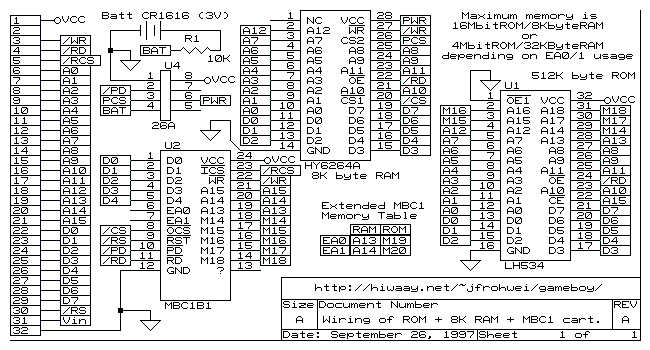
2nd future update would be to remove unnecessary routines like "shoot  " and "view" hopefully the ROM itself can be reduced in size. Potentially an MBC1 + SRAM + BATTERY
3rd future update I would like to break the ROM even more and remove saving altogether so that it can be safely put on a 64M cart along with LSDJ or a dedicated ROM only cart.

Tuesday, December 8, 2015

Composite Video from the Nintendo Gameboy

My latest project is to get some sort of video output from the nintendo gameboy. The signals are all present, but are not in a form that can be connected to any television or monitor. My first thought is to convert the signals into a single analog signal called composite video.

Composite video is named as such because it contains color data (chroma), brightness (luma) and synchronization on wire.

1. Chroma is not important in this case becuase the gameboy is monochrome. All of the color differences will be made with Luma.

2. Luma: As above, the Luma will be used to create our four different colors. The TV looks for an analog signal here. The gameboy has two data pins which are used for this purpose, so connected through a DAC of some sort, we can create four different levels rather than just 0v and 5v.

3. Sync
 Csync or composite sync is an XOR of horizontal and vertical sync. These two signals tell the television to move down one line or to move back to the top of the screen. I am not quite sure how progressive or interlaced are determined by these just yet.

Next, these have to be connected together over one wire. As mentioned, the luma is an analog value but what I forgot to mention was that it is a positive signal whereas sync is negative. From what I have read, composite must be AC coupled because the TV input is DC coupled. That being said, our sync can actually be positive as well, as long as the luma is offset by DC value. Once the signal goes into the TV, the DC coupling circuit will block the average DC offset which is our black level. Black level will become 0 volts inside the Tv so sync will become 0v to -0.4v and Luma will be between 0v and +0.7v.

I am not at liberty to share my schematic at this point but it doesn't' work that well anyhow. :P
As a first attempt however, the result is quite promising.

You will notice that the image scrolls in several directions and that it is repeated three times over from left to right. I believe this is a problem with synchronization and possibly the LCD itself.


Updates to follow shortly. 

Thursday, February 6, 2014

The Nintedno Gameboy Pocket's CPU pinout

I finally got around to probing the pins on the gameboy pocket's CPU and made a diagram. The CPU is not the same as the CPU inside of the original gameboy or the super gameboy SNES cartridge. When I get the chance, I will draw a schematic of the entire gameboy pocket.

Pinout photo direct link (huge): http://imageshack.com/a/img835/3936/nyix.png

  1.  A0
  2.  A1
  3.  A2
  4.  A3
  5.  A4
  6.  A5
  7.  A6
  8.  A7
  9.  A8
  10.  A9
  11.  A10
  12.  A11
  13.  A12
  14.  A13
  15.  A14
  16.  A15
  17.  D0
  18.  D1
  19.  D2
  20.  D3
  21.  D4
  22.  D5
  23.  D6
  24.  D7
  25.  /RES
  26.  VIN
  27.  SO1
  28.  SO2
  29.  MD7
  30.  MD6
  31.  MD5
  32.  GND
  33.  MD4
  34.  MD3
  35.  MD2
  36.  MD1
  37.  MD0
  38.  SOUT
  39.  SCK
  40.  SIN
  41.  CPG
  42.  CPL
  43.  ST
  44.  LD0
  45.  LD1
  46.  CP
  47.  FR
  48.  S
  49.  MA0
  50.  MA1
  51.  MA2
  52.  MA3
  53.  VCC
  54.  MA4
  55.  MA5
  56.  MA6
  57.  MA7
  58.  MA12
  59.  /MCS
  60.  MA10
  61.  /MRD
  62.  MA11
  63.  MA9
  64.  MA8
  65.  /MWR
  66.  CK2
  67.  CK1
  68.  P15
  69.  P14
  70.  P13
  71.  P12
  72.  GND
  73.  P11
  74.  P10
  75.  GND
  76.  GND
  77.  CLOCK-OUT
  78.   /WR
  79.   /RD
  80.   /CS

Some notes:

  • The naming convention that I followed is directly from the silkscreen on the gameboy pocket itself. 
  • It would seem that the gameboy pocket's CPU has the video RAM built-in as opposed to being on the PCB since the vram buses are all hanging open. Because of this, rewiring a DMG-01's CPU or a Super Gameboy CPU to the gameboy pocket is not immediately possible. 
  •  The DMG and SGB CPU's have two pins named T1 and T2 which are tied to ground. I believe that pins 75 and 76 of the MGBCPU  are T1 and T2 respectively, but only because of their placement near the clock output. 
  • The "/" means low-enable
  • For more information what some of the pins do, see the photo near the top. Or comment below.

Thursday, January 16, 2014

Jazz Disassemblies Ep4: N64 Gameboy Adapter Teardown

Some time ago, I needed the shell and cartridge connector of the gameboy adapter for the Nintendo 64, but I never throw things away. In light of this, I decided to de solder all of the components and write up a pinout diagram of the internal CPU itself.

This CPU is an 80-pin SMT IC just like the Original Gameboy, gameboy pocket and super gameboy however I am sure that it is more similar to the gamboy Color's CPU because of the abilities.

During my time desoldering everything, I forgot to record what components were so I no longer have that information. I would not have known some of the tiny transistor-like components anyhow because they had no markings.

In any case, I just want to share some photos with close ups of the traces and also the pin diagram.
Check it out:


I feel like I cheated on this dissassembly, because I have so little information. Sorry about that, I will just have to make the next one twice as in depth.

Thursday, November 14, 2013

Jazz-Assembly #2 - Yup, Another ArduinoBoy

Everyone and their mother has made one, so what took me so long? I have built them before, but this time I designed a PCB. What differs between mine and anyone else's is that I used economical parts rather than a pre built Arduino or an Atmega pulled form one with a bootloader.


Image Hosted by ImageShack.us

The entire board is a tiny 5cm x 5cm, MIDI connectors and LEDs included. I also plan on designing an acrylic shell to sell along side them, though anyone may choose to house it in their own enclosure.

Anyhow, this was the first time I had used SMT components besides an IC. Passive components including the resistors and caps were a new item for me to tackle. They did not challenge me as I had hoped. At one point, I blew one away from the pads, but it was all too easy to fix.

Image Hosted by ImageShack.us

Image Hosted by ImageShack.us

Image Hosted by ImageShack.us

Below is a shot for size comparison. You may have noticed in one of the photos that there is a notch on one side with a hole about 2 millimeters from it. This will be used for a zip tie so that I can ensure the cable does not break free. I will upload another picture once I complete that portion.

Image Hosted by ImageShack.us

Below is the wiring that I used to program both the flash and fuse bits. It is the same Bit Bang connection as we used on my version of the Gameboy Programmer board in a previous post. I found that the fuse bits were the most difficult to figure out in the whole project. in the end, I decided just to copy the fuse bits from a Pro Mini 5v/16MHz because that is what configuration I went with here.

Image Hosted by ImageShack.us

Thanks for reading. All credits for the ArduinoBoy go to Trash80 (Timothy Lamb) as can be found here:
https://code.google.com/p/arduinoboy/

Friday, October 11, 2013

Gameboy MBC - Which to choose?

Just a quick overview for unfamiliar readers before we get into the thick of it.

The Nintendo Gameboy uses a Memory Bank Controller inside of official cartridges for switching between banks of memory and ultimately expanding the addressable memory. The MBC will switch between banks of both ROM and RAM so that the programmer may code larger games and backup more data in save files.

There are four main MBC's numbered 1 through 5 and excluding 4. The reason I am writing this is because each following revision did not simply add more addressable memory. Each one has unique capabilities built in as well as expanding the addressable memory. in general the MBC's function by waiting for specific data bits to be written to yet more specific memory locations. Once the data in question is written to the specific memory location, the MBC switches the active bank of ROM and RAM to accommodate more code.
I will summarize each MBC as well as quote some information from datasheets.

MBC1


Is the first in the series of controllers which did only expand the addressable memory. Since the gameboy has 16 address pins and 8 data pins running through to the cartridge, the gameboy may without an MBC address only read from and write to a maximum of 256Kbits or 32Kbytes which is incredibly small considering Mario Land has 12 massive levels with multiple means of gameplay including the platformer and shooter, in both an airplane and submarine. Some of these levels even have secondary underworlds where Mario drops to an extra map off screen to collect secret coins or other items.

In any case, the MBC1 has two different modes to choose from. There is the 16Mbit ROM/8KByte RAM and 4Mbit ROM/32KByte RAM. 

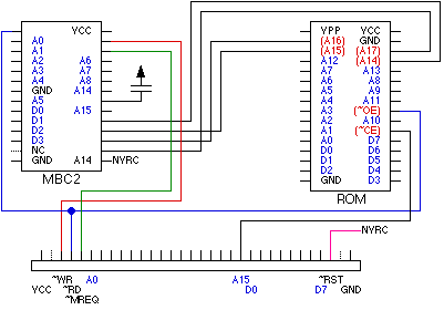
Note: RAM is an external IC which needs to be connected to a battery while disconnected from gameboy power to retain data.

MBC2

Similarly to the MBC1, the MBC2 maps extra banks of memory with specific memory writes; however, it may only map up to 2Mbits or 256Kbytes of ROM. Why a decrease? Well the magical thing about the MBC2 is that it contains 512 x 4 bits of SRAM built into the IC itself. This saves a lot of room on your cartridge board granted you are designing one.

The MBC2 can save money on RAM and space on your board if you are programming a small game that requires little ROM and RAM. Referring to the MBC1 above, if you wanted to offer a saving feature, you would need to source a RAM IC as well and route all of the Address, data and control pins to another location on the board.

MBC3

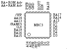
The MBC3 may again address up to 16Mbits of memory, but has a major feature built like the MBC2 has RAM. The MBC3 has an RTC or Real Time Clock built in. The RTC while still needing battery power when disconnected, offers a real-time count so that games such as pokemon may tell whether it is night or day, or when an hour in real life has passed for example.

Some games use the MBC3 without utilizing the RTC, but games that do include Pokemon of Generation 2 and Harvest Moon.

MBC5

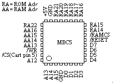
Lastly, the MBC5 is the final Memory Bank Controller from Nintendo. This particular MBC does not come with internal RAM or an RTC. It simply maps huge amounts of memory. It may map up to 64Mbits of ROM and up to 1Mbit of RAM but not both. There are different configurations to choose from; these are just the maximums.

This MBC which I find in nearly every Gameboy Color cartridge regardless of ROM size is guaranteed to work with the GBC's double speed mode. The others seem to work just fine too though, considering any GB game will run on your GBC.

For more information on how to use the MBC's with software, please refer to "Cartridge Types" in this document:
http://www.devrs.com/gb/files/gbspec.txt

MBC CPLD Clones & Reproductions

Aside from the Official Nintendo MBC's, people have had major success in recreating them using CPLD's. Both Homebrew developers and Chinese pirating companies that is.

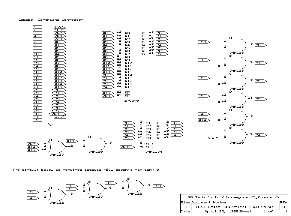
Since the MBC2 and MBC3 contain separate ICs, recreating them is much too difficult for a single person. MBC1 and MBC5 on the other hand can and have been redesigned by using CPLD's. They way they work as mentioned above is that they look for specific data bytes to be written to specific address locations. This Logic can be entirely drawn out using logic gates, which in turn can be programmed onto the CPLD.

MBC1 - CPLD

The MBC1 being the most simple, can be drawn using as little as 11 gates! (granted you do not need RAM)


MBC5 - CPLD

The MBC5 is much more complex of course, but it has also been cloned successfully by at least two separate people using two different CPLD's. One person used the XC9536 and the other person used the XC9572.

XC9536
http://chipmusic.org/forums/topic/2988/mbc5-clone-in-cpld/
and XC9572
http://home1.stofanet.dk/hvaba/gameboy/mbc5cpld/cpldcart.html

Depending on the number of inputs and outputs, more complex logic ought to be designed using PLD's or CPLD's. Not only can you save money on IC's, but space on your circuit boards. More often than not, a logic IC will take up space on your board and have a handful of unused pins and gates which is wasteful and lazy.

As always, thanks for reading! I hope I opened someone's eyes to new and old hardware.
Cheers

Wednesday, September 25, 2013

Using the Gameboy Programmer Board

Granted you have either bought a complete board from me or followed my DIY setup guide to a 'T', you are ready to use your Programmer/Reader board.

You'll need the software for the PC-side communication. You can find it on the author's site here:
http://www.reinerziegler.de/readplus.htm#Home made programming systems

Click the link "GB Cart Flasher programming software V1.1" and download the files. Install it where ever you like. If you are using Windows 7, you may need to run it in compatibility mode for Windows XP. I do and it works. If you don't know how to do that, right click on the shortcut and click properties, then check the box for compat mode and choose Windows XP. Then hit OK.

Image Hosted by ImageShack.us

Ready!

READING DATA

Plug in your device and then start the program. I like to make the window larger because there is a readout of what is happening. The readout should state that the program has started, whether it finds the device and then what firmware version is running on the device.


Image Hosted by ImageShack.us

Plug in a cartridge and hit "Cart info" to make sure that the cart has a proper connection. If everything is unknown and there is no "--ROM/FLASH content information" then remove your cart, clean the contacts and try it again.

Eventually, you should get a good connection and it will look something like this:


Image Hosted by ImageShack.us

take this info and set the boxes on the left to reflect it. In this case, we can see that the ROM is 512KBs, the RAM is 8KBs and the MBC is MBC1. It may not be necessary, but I will change the MBC to MBC1 rather than Auto just to be safe. Set those boxes, hit "Read Flash" and designate a save location.

The progress bar starts moving and the readout states that it is reading. After a time depending on the ROM size, you'll see ">Success!" Follow the same method to backup your save files but hit "Read RAM" instead.

Image Hosted by ImageShack.us

As you can see above, I backed up both files. Save files are not compatible with all emulators, but they are good to keep on hand since the internal batteries are dropping like flies now-a-days.


Image Hosted by ImageShack.us


WRITING

The method to write ROMs and RAMs is the same, but just with two different buttons.
Plug in your "flashable" cartridge and click on "Cart Info" again. You'll either be given the contents as before or you'll be given the "Cartridge is blank, damaged or not connected" message. Hopefully, it is just blank. ;)


Image Hosted by ImageShack.us

In any case, hit "Erase FLASH" and wait for the process to complete, otherwise you will get a timeout error if the ROM is already full.


Image Hosted by ImageShack.us

Once it succeeds, press "Write FLASH" and browse for your ROM. It will go through the process and complete.


Image Hosted by ImageShack.us

Thanks for reading and Enjoy your gameboy!
~Jazz

Sunday, September 22, 2013

Populating the GB-Programmer (Jazz-Assembly #1)

The board has been designed to accommodate different methods of programming the Atmega8515 (hereby simply called 8515). Once programmed, you may never choose to reprogram it again because there may never be updates to the firmware anytime in the future.

Step 0.
Admire your beautiful new toy. 

It shall prove to be very useful regardless of your individual purposes. Also, at no time should you power your board until I say so.

Step 1.
Soldering both SMT ICs

The picture below is of two board prior to me cutting them apart. To reduce cost, I panelized my design.


Image Hosted by ImageShack.us

You may choose to solder one IC at a time or both at once depending on your skill and resources. It would be highly suggested to use either a hot air gun or some type of oven and solder paste. Soldering by iron is perfectly possible, but creates more chance for failure. If you are a frequent reader, you should know that I now own an awesome hot air station, so I also bought a tube of solder paste.

Simply apply a very small amount of solder paste to the bare pads and carefully place your IC over top of them. Make sure that it is aligned as closely as possible, not forgetting to orient pin 1 in the right direction. Pin 1 is designated by the white circle on the board.

Image Hosted by ImageShack.us

Image Hosted by ImageShack.us

Once you finish both ICs, make sure that there are no shorts in places that they may not be. If you find one, attempt to draw the solder off of the pins with your iron or solder wick. Check it again and once satisfied, move on.

Step 2.
Through-hole components.

As much as I had hoped not to use any through-hole components, my audience insisted. The through-hole components required include:

2x 0.1uF ceramic capacitors (may be labelled 104)
1x 4.7uF electrolytic capacitor
1x 10K ohm resistor
1x 1K ohm resistor
2x 220 ohm resistors
2x LEDs (two colors)
1x female USB type B connector
1x gameboy cartridge connector

For the time being, do not populate C4, R6 and R7. These are not relevant at this time. You may choose to use a 6MHz ceramic oscillator, but I suggest saving the money and moving on. If you do though, cut the trace leading from it to the FDTI chip.

Start by placing the leads into the holes and bending them away from center so that they stay in place. Sodler each component on the underside and clip the legs at the board. Some people would suggest to clip them before soldering though.

Also make sure that the electrolytic capacitor (C3) faces negative lead down as shown below. Each components has the appropriate value marked on the board, so you cannot go wrong. Seating the gameboy cartridge connector may be the most difficult through-hole component. It has the most pins and each of these pins could be slightly bent from originally removing it. Take your time and do not stress.

Image Hosted by ImageShack.us

The LEDs can be any color you like, but know that the one farthest from the resistor is power and the other one is activity. I prefer my toys to have a green power LEd. ;)

Image Hosted by ImageShack.us


Step 3. 
PC Connection

Check your SMT soldering ONE MORE TIME. If and only if there are no shorts between pins, connect the board to your PC and cross your fingers... IF all is well, the LED should light up and a driver should automatically install for your device. It will also be given a COM port number.


Image Hosted by ImageShack.us

Step 4.
Programming the FT232RL and 8515

Thats right, you're going to program both ICs. There is only one modification that needs to be made to the FT232RL (hereby simply called 232) which is to make it output a 6 MHz clock rate. This is for the 8515 to run on.

First, the 232's internal eeprom must be modified. To do this, we will use FT_Prog found on the FTDI website here:
http://www.ftdichip.com/Support/Utilities.htm#FT_Prog

Only one modification must be made and that is to change the CBUS0 pin to act as a 6 MHz clock. We will not worry about the other pins because they are all unconnected. CBUS0 is one of five programmable I/O pins and there are many options to choose from, but I am not going to cover these here.

Install FT_Prog and run it. You'll be greeted by a well designed GUI ... just don't touch anything. plug in your device and it should install a driver if it has not already. Once "Your device is ready to use" go ahead and click "Scan and Parse" which looks like a magnifying glass. Your device should pop up in the dialog box under device tree like this:

Image Hosted by ImageShack.us

You can see that your device is already programmed, but we must now change one function. Expand the device tree as such:
FT EEPROM -> Device Specific -> IO Controls -> C0
Use the drop-down to select CLK6 in the C0 bus only. The other pins are all useless as they are not connected to anything. Ignore them.

Image Hosted by ImageShack.us

Click on the lightning bolt which is the program button, make sure your device is selected and press "program" if and only if you are positive you did not change any other settings.
The bottom of the window will say finished and then ready. Close the window and close FT_Prog, then disconnect your programmer.

Image Hosted by ImageShack.us

Reconnect your device once more and it should install the drivers again and give it a new COM port. You can now move on, but if you were to open your device in FT_Prog again, you would notice that C0 is still set to CLK6. Good job!

Just a note, but the reason you should not touch any other options in the eeprom settings is because there are too many settings that can be set incorrectly. For example, if you were to program your device to use an external oscillator, it would be rendered useless and you spent a lot of time and energy soldering that chip perfectly! So be careful!

Step 5.
Programming the 8515.

The easiest way to program the 8515 is via FTDI BitBang. It is a totally new concept to me, but incredibly useful considering how much people want to charge for ordinary ICSP programming kits. It may be a tad bit slower at programming, but since you will only program the 8515 once, it does not matter.

I put together a file-pack to get you started. This pack  includes AVR_DUDE, my custom config file special for this programmer and the hex file which needs programmed to your 8515. I am writing the guide on the GUI version of AVR-DUDE. Everything is easier with a GUI, though you have to show a little love for the tried and true command prompt. ;)

Download it here:
http://www.noisechannel.org/wp-content/uploads/2013/09/GB-Progger-kit.zip

Lets get started.

Go ahead and hook up your programmer if it is not already. Open avrdude-GUI.exe.
1. Direct the first box to your avrdude.exe
In our case, we will be using the avrdude-serjtag that you downloaded.
2. Pull down the "Programmer" Box and select the "FT232R Synchronous BitBang for Jazz (GBProgger)."
3. Leave the port drop box blank.
4. Locate "ATmega8515 (m8515)" under the "Device" drop-down.
5. Type "-P ft0 -B 4800" in the "Command line Option" box. It should look just like this below:


Image Hosted by ImageShack.us

6. Click the "Read" button under Fuse. This will show you the fuse bits on your 8515 which must be changed. It does not matter what they are now.


Image Hosted by ImageShack.us

7. Change the fuse bits to C910 as pictured and hit write. It will be very fast and just ask you if it went well.


Image Hosted by ImageShack.us

8. Now erase "-B 4800" from the "Command line Option" and browse for the hex file under Flash then hit write. It is also fast, too fast for me to get a screenshot even.


Image Hosted by ImageShack.us

9. Exit and done. Disconnect your device and reconnect it. If all went as planned, you now own a GB Programmer and Dumper for whatever needs you may have.

Lets test it out, shall we? That is another blog post, for another time. See you then! :D

 Cheers,
Jazz

Tuesday, September 17, 2013

Gameboy Cartridge Reader Update

It has been a long and wonderful journey since the beginning of this project and if given the chance, I would do it all over again. For any readers who did not purchase a board, we are closing in on the end of the project. All of my boards and parts have arrived and I am simply pumping out completed board one after the other. Surface mounted components are very easy to do granted you have a hot air station, which I clearly do! Now that I have a little practice on the machine, SMT components take less time than through hole components. An FT232RL chip takes me less time to solder than a Through-hole resistor! Who would have guessed?

Anyhow, I know that all you're waiting for is pictures, so here they are:
In rough order from delivery to completion.

  Image Hosted by ImageShack.us

Image Hosted by ImageShack.us

Image Hosted by ImageShack.us

Image Hosted by ImageShack.us

Image Hosted by ImageShack.us

Image Hosted by ImageShack.us

Image Hosted by ImageShack.us

Image Hosted by ImageShack.us

Image Hosted by ImageShack.us

Image Hosted by ImageShack.us

Image Hosted by ImageShack.us

Image Hosted by ImageShack.us

Image Hosted by ImageShack.us

Wednesday, August 21, 2013

Making Gameboy Sprites, Tiles and Maps

Just to put it on the table, you have no business creating anything for Gameboy if you have not yet read "Everything You Always Wanted To Know About GAMEBOY: but were afraid to ask."

Read it and then return for my tutorial. I can wait.

***

Now then, lets start talking about sprites, maps and other graphic elements. As you very well know, the Dot matrix gameboy displays four shades of grey (or green). Each shade is represented by two bits: 00, 01, 10 or 11 respectively. It isn't that important to know right now, but while setting up the palette in your gameboy code, it is commonly done as follows:

...
init:
ld a, %11100100 ; Window palette colors, from darkest to lightest
ld [rBGP], a        ; Load Accumulator A (11100100) into rGBP
...

Where "rBGP" Equates to $FF47, an address representative of the specially reserved I/O Register...but why am I just repeating what you have already read, right?

Now, back to the point. You may choose to design all of your characters and objects for your game strictly in binary or hexadecimal data if you wish but I prefer the visual approach. You know, the kind with a GUI. ;)

First download these two programs:
Gameboy Tile Designer: http://www.devrs.com/gb/hmgd/gbtd.html
Gameboy Map Builder: http://www.devrs.com/gb/hmgd/gbmb.html

Both of these tools will help you create and visualize the output of tiles and maps. Tiles are going to be used both for maps and for sprites, you can imagine a sprite or character figure to be a collection of tiles. Pretty simple.

You'll start by opening  Gameboy Tile Designer (or GBTD.exe). I like to keep the default color palette which is "Gameboy Pocket" because it is easier to work in shades of black rather than shades of green. Under View, I also like to switch to "simple" and use nibble markers, though they are not very easy to see. 

Image Hosted by ImageShack.us

Next select the color you would like to draw with by adding it to either your left mouse button or right mouse button by clicking on it with the corresponding button. Start filling in squares to your liking. You make design single 8 x 8 sprites or larger. Anything you wish as long as it is four colors. Once you finish a tile, click on the next blank tile on the far right of GBTD.

Image Hosted by ImageShack.us

You will save the file with whatever content you have at this point and name it something relative to the content. Open Gameboy Map Builder (or GBMB.exe) and click file > Map Properties then use the browse button to locate your new *.GBR file that you made in GBTD. For no, you may ignore width and height because you can add columns and rows at will.

Image Hosted by ImageShack.us

Once you have loaded in your tiles, you may continue to make more tiles! Make and place tiles, side-by-side by having both programs open at once. Each time you save your *.GBR file in GBTD, GBMB will automatically update! How cool is that?

Here are some time-elapsed screenshots of my own work.


Image Hosted by ImageShack.us

Image Hosted by ImageShack.us

Image Hosted by ImageShack.us

Image Hosted by ImageShack.us

Image Hosted by ImageShack.us

Image Hosted by ImageShack.us

Image Hosted by ImageShack.us

The above Map is simply a 160x144px image that I can manipulate on screen. REMEMBER:
"The main GameBoy screen buffer (background) consists of 256x256 pixels or 32x32 tiles (8x8 pixels each). Only 160x144 pixels can be displayed on the screen." That means that where ever I place the image on the gameboy, there will be large empty scape on the sides. If I wanted to, I could have designed a full 256x256px map and used a scroll option and the d-pad buttons to view it all.


My process of designing such a large map was that I took an image I had re-sized and pixelized in Photoshop. There are a few options when pixelizing and for this one, I chose "pattern."

Below is the full 160x144 image which I have then transposed into GBTD...one tile at a time. It took nearly four hours, but I figured out that I was able to copy and paste a few of the colors. It turened out that the three lightest colors could be copied and pasted from PS to GBTD. I still had to fill in the black (11) pixels though.

Image Hosted by ImageShack.us

Image Hosted by ImageShack.us

Image Hosted by ImageShack.us

With a temporary frame, I was able to see more clearly which pixels I was currently working on. Again, I did this one 8x8 tile at a time.

Once you get better at creating tiles, you can create all sorts of maps and sprites, both for game characters and even art!

Image Hosted by ImageShack.us

When I am able to write better ASM code, I will demonstrate how to export these files and INCLUDE them into your very own ROM images. Thanks for reading!