Showing posts with label guide. Show all posts

Sunday, December 13, 2015

ROM, EPROM, EEPROM that I like

Here is a quick-check list of different roms that are easy to get.
All run on single supply voltages of 5v and are accessed via a parallel bus.
Also listed is what to do with those pesky control pins when if you just want these to be read by the controlling system (NES, Genesis, z80, etc)

8-bit UV Eproms:

27c16 - 2,048b x8 = 2 KBytes 
27c32 - 4,096b x8 = 4 KBytes
27c64 - 8,192b x8 = 8 KBytes 
27c128 - 16,384b x8 = 16 KBytes
27c256 - 32,768b x8 = 32 KBytes
27c512 - 65,536b x8 = 64 Kbytes

8-bit EEPROMs:

29f010 - 131,072b x8 = 128 KBytes alt: 29ee010, 49f010
29f020 - 262,144b x8 = 256 KBytes alt: 49f020
29f040 - 524,288b x8 = 512 KBytes alt: 49f040

8- or 16-bit UV EPROMs:

27c400 - 512Kb x8 or 256Kb x16
27c800 - 1Mb x8 or 512Kb x16
27c160 - 2Mb x8 or 1Mb x16
27c322 - 2Mb x16 (no 8-bit mode available)

8- or 16-bit EEPROMs:

29f200  -  256Kb x8 or 128Kb x16 (~1.64usd ea)
29f400 - 512Kb x8 or 256Kb x16 (~2.11usd ea)
29f800 - 1Mb x8 or 512Kb x16 (~3.12usd ea)
29f160 - 2Mb x8 or 1Mb x16 (price unknown)

8-bit EEPROMs I am looking into:

29- or 49-f040  - 512Kb x8
29f080  -  more info once I use them
29f016
29f032

There are of course hundreds of other roms, but I don't use them.

Control Pins:

None of these pins can be left hanging (disconnected) as far as I know. So don't do it.
Note: "!" will be used to distinguish low-enable pins. This means that when this input is pulled low, the function is enabled.

!CE - Chip Enable, AKA !E:
Most likely your system will need this to be connected to the control bus of the system. Sometimes it is connected to GND directly if your system has NO other memory that it must address. Sometimes it is connect to !OE, but only if your system has no other memory to access.

!WE - Write Enable. AKA !WR:
Typically your system will not be able to program the rom, so this should be pulled high by a resistor connected to vcc. Sometimes you can get away with connecting this pin directly to vcc without a resistor. Anywhere between 4k7 to 10k ohms should be good.

!OE - Output Enable. AKA !RD, !G:
Most likely your system will need this to be connected to the control bus of the system. Sometimes it is connected to GND directly if your system has NO other memory that it must address. Sometimes it is connect to !CE, but only if your system has no other memory to access.

!PGM - Program Enable:
This is similar to !WE but is only seen on a select few ROMs that also require a VPP voltage. Connet this pin to vcc inside your system.

VPP - Programming voltage:
This is typically a high voltage of 12v to 21v required to program a UV EPROM. This is not going to be used by your system, so it should always be pulled high/VCC/+5v.

!OEVPP - Output Enable / Programming voltage
When low (0v), this pin acts as the data output enable pin. When high (vcc) this pin shuts off data output. When connected to vpp (typ. 12v - 21v) this pin acts as vpp putting the chip into programming mode. Connect this pin to your control bus as though it were just !OE.

Q15A-1 - This pin is very special! When in 16-bit mode (byte pin high), this pin is used as data pin D15 or Q15.When in 8-bit mode (byte pin low), this pin is Address pin minus 1. And yes, by minus 1, this is less than 0. What that means is, the pin will connect to A0 on your computer's bus, eprom pin A0 will then connect to computer side A1, etc. here is a little diagram:

rom ---- computer
A-1 ---- A0
A0 ----- A1
A1 ----- A2
A2 ----- A3

!BYTEVPP - Byte Mode / Program Supply:
This pin is pulled high if using the rom in 16-bit mode, or ground when in 8-bit mode.
When this pin is connected either to VSS or VCC, then VPP is ignored, The only time the VPP function is used is when the voltage connected is 12v to 21v as instructed by the appropriate datasheet.
Further explanation from a datasheet:

The M27C160 (for example) has two organisations, Word-wide and Byte-wide. The organisation is selected by the signal level on the BYTEVPP pin. When BYTEVPP is at VIH the Word-wide organisation is selected and the Q15A–1 pin is used for Q15 Data Output. When the BYTEVPP pin is at VIL the Byte-wide organisation is selected and the Q15A–1 pin is used for the Address Input A–1. When the memory is logically regarded as 16 bit wide, but read in the Byte-wide organisation, then with A–1 at VIL the lower 8 bits of the 16 bit data are selected and with A–1 at VIH the upper 8 bits of the 16 bit data are selected.

For a much more in-depth explanation of eproms, see:
https://wiki.xtronics.com/index.php/How_EPROMS_Work


Wednesday, June 4, 2014

Repairing an LCD Monitor

I am damn cheap, and this isn't the first time I have gotten a broken monitor to use as my own. By broken, I do not mean that the LCD is cracked, but that it comes on and goes off immediately. Some even went black and had a buzzing noise. More often than not, this means some capacitors on the power board are swollen or popped. This is just a detailing of one monitor in particular, but the method is nearly identical to other modern screens. The other problem that could occur seems less common, so I will not cover it here. The less common problem is the wires connecting to the CCLF tubes coming loose.

Step 1. Open the screen.
Unplug the monitor and press the power button a few times to (mostly) discharge any good capacitors.
Find all of the screws that are visible including VGA/DVI mounting screws and remove them, keeping a good idea of which holes they came from.

Now pry apart the plastic shell carefully. I use an expansion slot cover found on the back of a PC because they are wider than a screwdriver and leave less cosmetic damage (if any at all). Once you have the plastic bevel popped all around the edges, place the screen on your surface area, or lap, face down and lift the plastic off the back. This may not be the exact way for all monitors, but it has been for the last four I repaired.

Step 2. Take note of the orientation of the wires leading from the metal shielding. THese connecto to the high voltage CCFL tubes and may or may not be polarized. Don't screw this up! Take a photo if it helps.


Remove the metal shielding from the power and logic boards. Be very careful of any ribbon cables.
You should find the power board which is suspect.


Step 3. Inspect the power board. If you find swollen capacitors, you probably found the culprit. In our case, there are two swollen capacitors. From my experience, they normally go out in pairs, but I cannot prove that. Can you see the two fatties?


Step 4. Replace the capacitors with a "good" brand. Nichicon is my favorite. Make sure that the Farads are matched exactly and that the voltage is either the same or higher. Higher is better in this case, but normally the caps become larger with a higher voltage tolerance.


Step 5. Put it back together and power it up. ta-da! Although this is not 100% to work for you, it is a common problem and an easy fix. Good luck and good modding.

-Jordan

 ps. The monitor in this example was the Westinghouse L1975NW. I replaced two 220uF 25v capacitors with two 220uF 35v capacitors.
I also repaired an Acer x193w+ with new caps and some other Acer I no longer have.
One time I found that a Dell E2K-SE198WFPF(B) by reconnecting the CCFL tube with its wire which was difficult and apparently dangerous. To do so I had to disassemble the screen itself, LCD, polarizing film, and other layers just to get at the tubes...which were well encased in rubber. It was very difficult and I don't think that I would attempt it again.

Wednesday, April 23, 2014

Adding Analog Pins to Arduino pt.2

Don't forget part 1: http://jazz-disassemblies.blogspot.com/2014/01/adding-analog-pins-to-arduino-pt1.html

The first step in part 2 of adding analog pins to an arduino is by getting rid of the MCP3008! Yes, I am sorry but that particular IC is overly complicated and too expensive for what it offers.

Since I wrote that first part, I began looking for alternatives because of the price of the MCP3008. Even in quantities of 10 or more, the IC was still more expensive than a bare Atmel microcontroller! At first I thought that I could buy another microcontroller for less than the MCP3008 at a fraction of the cost and even be able to simplify the methods of communication to my own liking.

After looking for the cheapest, yet adequately powerful uC, I came across the ATtiny48 which has several Analog inputs and even more digital IO's. The Analog inputs would in theory, be read, stored in variables and then transferred to the master microcontroller across an 8-bit wide data bus. The particular analog value that would be transferred would be selected by the master uC via three other pins; select bits. The pins were going to offer a binary value which would select the current pot to be transferred.

This method would allow for me to read many many more pots than the master microcontroller was equipped with, but at a large cost; the cost of many digital IO pins. One way to get those digital IOs back would be to use analogWrite on one of the PWM outputs and connect that pin to an analog input on the master uC. Considering that, I could sacrifice one analog input for 8 more. HOWEVER, the AT48 has no PWM outsputs. :(

After mulling over it for a long time, I realized what I had actually designed. The program I had spent an hour writing... The program that utilized the exact methods of communication to suite my exact needs...was, you guessed it: An analog multiplexer which decodes 3-to-8 inputs. They have an app...I mean IC for that. The 74HC4052 accepts two sets of 4 analog inputs and connects them to one of two outputs respectively. Two select bits, choose the analog input to transfer to the output.

The 4052 is a mere 50 cents, requires no external programming, runs on a large voltage range and comes in a variety of packages!

I will simply import photos and descriptions of my project, so that I can describe how to use the 4052.
Analog pins A0-A3 are used for higher priority data, so that leaves A4-A7 open. Again, we will also need two digital IO to use as select bits on the 4052.

// ***************************************************************
// define pin connections
// ***************************************************************

int pSelect0 = 3;
int pSelect1 = 4;

// ***************************************************************
// define variables
// ***************************************************************

// locate the delay between the select bits and the updated output
// of your 4052 IC and update this value:
int latency = 100; 

byte aVal00 = 0; // analog Value, 4052 # 0, input 0
byte aVal01 = 0; // analog Value, 4052 # 0, input 1
byte aVal10 = 0; // analog Value, 4052 # 1, input 0
byte aVal11 = 0; // analog Value, 4052 # 1, input 1

byte aVal02 = 0; // analog Value, 4052 # 0, input 2
byte aVal03 = 0; // analog Value, 4052 # 0, input 3
byte aVal12 = 0; // analog Value, 4052 # 1, input 2
byte aVal13 = 0; // analog Value, 4052 # 1, input 3

byte aVal04 = 0; // analog Value, 4052 # 0, input 4
byte aVal05 = 0; // analog Value, 4052 # 0, input 5
byte aVal14 = 0; // analog Value, 4052 # 1, input 4
byte aVal15 = 0; // analog Value, 4052 # 1, input 5

byte aVal06 = 0; // analog Value, 4052 # 0, input 6
byte aVal07 = 0; // analog Value, 4052 # 0, input 7
byte aVal16 = 0; // analog Value, 4052 # 1, input 6
byte aVal17 = 0; // analog Value, 4052 # 1, input 7

// ***************************************************************
// Setup
// ***************************************************************

void setup()
{
Serial.begin(9600);
// define pin modes   
pinMode(pSelect0, OUTPUT);
pinMode(pSelect1, OUTPUT);
}  

// ***************************************************************
// Main Loop
// ***************************************************************

void loop()
{
getAnalog();
processAnalog();
}

// ***************************************************************
// Get Analog Values
// ***************************************************************

void getAnalog()
{

  // read the first set of four
  // part 1 of 4
  digitalWrite(pSelect0, LOW), digitalWrite(pSelect1, LOW); // 00
    delayMicroseconds(latency);
  
aVal00 = map(analogRead(A4), 0, 1023, 0, 255),
aVal01 = map(analogRead(A5), 0, 1023, 0, 255),
aVal10 = map(analogRead(A6), 0, 1023, 0, 255),
aVal11 = map(analogRead(A7), 0, 1023, 0, 255);
  
  // read the second set of four
  // part 2 of 4
  digitalWrite(pSelect0, LOW), digitalWrite(pSelect1, HIGH); // 01
    delayMicroseconds(latency);
  
aVal02 = map(analogRead(A4), 0, 1023, 0, 255),
aVal03 = map(analogRead(A5), 0, 1023, 0, 255),
aVal12 = map(analogRead(A6), 0, 1023, 0, 255),
aVal13 = map(analogRead(A7), 0, 1023, 0, 255);
  
  // read the third set of four
  // part 3 of 4
  digitalWrite(pSelect0, HIGH), digitalWrite(pSelect1, LOW); // 10
    delayMicroseconds(latency);
  
aVal04 = map(analogRead(A4), 0, 1023, 0, 255),
aVal05 = map(analogRead(A5), 0, 1023, 0, 255),
aVal14 = map(analogRead(A6), 0, 1023, 0, 255),
aVal15 = map(analogRead(A7), 0, 1023, 0, 255);
  
  // read the last set of four
  // part 4 of 4
  digitalWrite(pSelect0, HIGH), digitalWrite(pSelect1, HIGH); // 11
    delayMicroseconds(latency);
  
aVal06 = map(analogRead(A4), 0, 1023, 0, 255),
aVal07 = map(analogRead(A5), 0, 1023, 0, 255),
aVal16 = map(analogRead(A6), 0, 1023, 0, 255),
aVal17 = map(analogRead(A7), 0, 1023, 0, 255);  
  
  
  return; // return to main loop    
return;
}

// ***************************************************************
// Process the values
// ***************************************************************

void processAnalog()
{
// Do whatever you would like to do with the values here
return;
}

// ***************************************************************

That is all. I realize that the getAnalog function could be simplified using an array, but I did it quickly. If anyone wants to make that change, please share it! Also, I used the map function to change the analog value that was read from 10-bits to 8-bits. I have my reasons, but anyone may remove that if they want a higher resolution. 

There you have it. 16 independent analog values on top of the 4 I needed for something else. With all of the analog pins at our disposal, you could have 32 analog values! I am using this for 16 pots and the other 4 for external control voltages. Just imagine, 32 analog values with a simple Atmega168. 

Keep up with future posts to see when I actually breadboard this out. 

Thursday, January 23, 2014

Adding Analog Pins to Arduino pt.1

EDIT: I suggest reading this post instead:
http://jazz-disassemblies.blogspot.com/2014/04/adding-analog-pins-to-arduino-pt2.html
It is easier and more straightforward to program for.

All of the commonly used Arduino boards have Analog pins for use in converting analog data to digital data that can be manipulated via code. Arduino Pro Mini, Nano, Mega, Duemilanove, are all examples of boards that have 8 or more ADC pins and in some cases, they're not even all broken out!


In any case, 8 pins may not be enough for your needs, I know this fact first hand. The reasons why you may need so many ADC connections is not important, but figuring out a way around the problem is!

First, lets talk about know about the ADC pins before using them.
1. They may be used as Digital I/O.
2. They convert the analog voltages to digital data with a 10-bit resolution.
3. You don't want to waste them. ;)

The 10 bit resolution means that the data returned when using them as Analog inputs is within the range of 2^10, or 0 - 1023. I like to work with data in binary, but the data may be dealt with in decimal, binary or hex if you wish. Like:
B0000000000 - B1111111111
0x000 - 0x3FF
0 - 1023

Aside from the main point of this post, my needs are to use the values from potentiometers in an 8-bit resolution. I just found out that instead of shifting the data to the right twice (or divided by 2 twice) that the data range itself may be mapped to other values, both higher or lower. One way to read an analog input and mapping the value is as follows:


/*
Stupid simple code to read a pot value and map it to another range.
By Jazzmarazz

map(value, fromLow, fromHigh, toLow, toHigh)
*/

int A0pin = A0;

int potVal = 0;

void setup() {
pinMode(A0pin, INPUT);
Serial.begin(9600);
}
void loop() {
map(analogRead(A0pin), 0, 1023, 0, 255);
Serial.println(A0pin);
delay(500);
}

The map function could allow for you to map it to most any value:
map(analogRead(A0pin), 0, 1023, 0, 9);
map(analogRead(A0pin), 0, 1023, 0, 4095);
map(analogRead(A0pin), 0, 1023, 10, 100);
Whatever you like, for whatever purposes.

In addition, it is a good idea to read the constrain function:
http://arduino.cc/en/Reference/Constrain

Now to the point. To add many more ADC pins to the arduino, I suggest adding an external ADC via an SPI connection. Alternatively, you may use an I2C connection, but it seems like SPI devices come equipped with more analog channels. The MCP3008 for example, is an 8-channel, 10-bit ADC. This means that there are 8 analog inputs which all read back in the above mentioned 10-bit resolution.

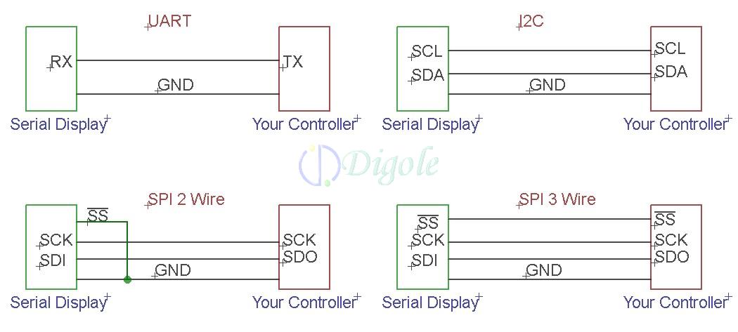
To wire one such device to our Arduino, we must follow one of the Communication methods:

UART, I2C, SPI 2 wire, SPI 3 wire and lastly, 4 wire (full) SPI. An example of all four connections are shown below. In all of these cases, you need at least two things, a master device and a slave device. In our case, the master is our Arduino and the slave will be the MCP3008 ADC. Below also shows how you can daisy chain more slave devices to the same master bus. This is incredibly helpful because all of the devices are going to share up to three of the connections, and only have one connection that is unique to itself.


The shared connections are SCK, MOSI, and MISO while the unique connection is SS, but what do these connections mean?

MISO (Master In Slave Out) - The Slave line for sending data to the master,
MOSI (Master Out Slave In) - The Master line for sending data to the peripherals,
SCK (Serial Clock) - The clock pulses which synchronize data transmission generated by the master and one line specific for every device:
SS (Slave Select) - the pin on each device that the master can use to enable and disable specific devices.

Pretty simple, taken straight from the Arduino reference guide. You're probably wondering where the pins are. Now, you can write your own functions if you wanted to drop the external SPI slave anywhere, but a custom code is going to be much slower and it would be more easy to move your other connections somewhere else so that these pins are free for SPI:


Digital pin 13 is the Serial clock, 12 is Master Input, 11 is Master output and lastly, SS or Chip enable is 10, but I believe this can be moved where ever since it just requires a digitalWrite high or low. Low to enable of course.

That is about as complicated as it gets, honestly. Now, back to my needs. To iterate, I need to read the analog values of many potentiometers to assign to other devices, not on the SPI bus. We can do this two ways. Wire up all four connections, or wire up three connections and tie SS to ground on the slave only. If we keep SS connected to the Arduino, then we can expand the SPI bus to have more devices, more analog inputs, sensors, outputs, etc. IF we tie SS to ground, then the slave will always be active but can be the only SPI device on our bus.

Looking at the datasheet, there are two package types, the 3004 and the 3008. Both will take up all of the same connections, so lets focus on the 3008.


Pins 1 - 8 are the Analog input pins where we will connect the wiper of our pots. Pin 10 is the 1CS pin, which we will connect to !SS on the arduino. Pin 11 is the Din or Data input pin which will be connected to the Dout pin of the Arduino, MOSI. Pin 12 is the Dout which will be connected to the MISO pin. and lastly, the clock pin on 13 will be connected to Digital pin 13 on the Arduino.

Pins 16 and 15 will be bridged and connected to VCC or +5v. VDD is the supply and Vref is the reference voltage that the analog inputs are referencing. If we had a lower vref like 3v3, then our pots would have to be connected between Ground and 3v3, while the IC runs on +5v.

Pins 14 and 9 are the two grounds, Analog ground and digital ground, respectively. This may be one of the more confusing parts to hook up if you over think it. Copied stright from the datasheet:

"Utilizing the Digital and Analog Ground Pins The MCP3004/3008 devices provide both digital and analog ground connections to provide additional means of noise reduction. As is shown in Figure 6-5, the analog and digital circuitry is separated internal to the device. This reduces noise from the digital portion of the device being coupled into the analog portion of the device. The two grounds are connected internally through the substrate which has a resistance of 5 -10Ω. If no ground plane is utilized, both grounds must be connected to VSS on the board. If a ground plane is available, both digital and analog ground pins should be connected to the analog ground plane. If both an analog and a digital ground plane are available, both the digital and the analog ground pins should be connected to the analog ground plane. Following these steps will reduce the amount of digital noise from the rest of the board being coupled into the A/D converter."


What this basically means is that having analog ground and digital ground connected together may cause interference in the form of noise on the data traces. Since most of our Arduino board have only a single GND pin, we will have to take separating the two into our own hands. Some suggest dividing the two ground planes by a gap and then connecting them together via a small bridge like so:


They also suggest that you use separate power supplies. You should also remember to route any traces crossing the ground planes trough the bridge and not over the gaps. Being so strict will help you to reduce noise, but how much noise do you think that you actually have in your circuit? Are you running it on an unregulated series of AA batteries? A potato (joke)? Could you not afford filter capacitors? In most cases, the on board Arduino regulator is going to do its job in regulating the power supply, reducing noise and with capacitors between VCC and GND, yet more noise reduction.

Unless you plan on wiring up many different crystal oscillators, high speed devices, and wireless communications all on the same board, then your noise should not be readily noticeable.

Now enough of my tangents. I made up a quick MSpaint drawing of the connections:


That is the wiring diagram we will use, but for the time being, the MCP3008's are still in the mail. Once they arrive, I will write part 2 where we actually wire up the circuit and write some code to read from each pot. You may notice that the pinout is exactly 13 -> 13, 12 -> 12, 11 -> 11 and 10 -> 10. It would seem that the SPI functions were written to accommodate common SPI pinouts. You may see this on other SPI devices as well.

Thanks for reading!
Part 2: http://jazz-disassemblies.blogspot.com/2014/04/adding-analog-pins-to-arduino-pt2.html

Wednesday, September 25, 2013

Using the Gameboy Programmer Board

Granted you have either bought a complete board from me or followed my DIY setup guide to a 'T', you are ready to use your Programmer/Reader board.

You'll need the software for the PC-side communication. You can find it on the author's site here:
http://www.reinerziegler.de/readplus.htm#Home made programming systems

Click the link "GB Cart Flasher programming software V1.1" and download the files. Install it where ever you like. If you are using Windows 7, you may need to run it in compatibility mode for Windows XP. I do and it works. If you don't know how to do that, right click on the shortcut and click properties, then check the box for compat mode and choose Windows XP. Then hit OK.

Image Hosted by ImageShack.us

Ready!

READING DATA

Plug in your device and then start the program. I like to make the window larger because there is a readout of what is happening. The readout should state that the program has started, whether it finds the device and then what firmware version is running on the device.


Image Hosted by ImageShack.us

Plug in a cartridge and hit "Cart info" to make sure that the cart has a proper connection. If everything is unknown and there is no "--ROM/FLASH content information" then remove your cart, clean the contacts and try it again.

Eventually, you should get a good connection and it will look something like this:


Image Hosted by ImageShack.us

take this info and set the boxes on the left to reflect it. In this case, we can see that the ROM is 512KBs, the RAM is 8KBs and the MBC is MBC1. It may not be necessary, but I will change the MBC to MBC1 rather than Auto just to be safe. Set those boxes, hit "Read Flash" and designate a save location.

The progress bar starts moving and the readout states that it is reading. After a time depending on the ROM size, you'll see ">Success!" Follow the same method to backup your save files but hit "Read RAM" instead.

Image Hosted by ImageShack.us

As you can see above, I backed up both files. Save files are not compatible with all emulators, but they are good to keep on hand since the internal batteries are dropping like flies now-a-days.


Image Hosted by ImageShack.us


WRITING

The method to write ROMs and RAMs is the same, but just with two different buttons.
Plug in your "flashable" cartridge and click on "Cart Info" again. You'll either be given the contents as before or you'll be given the "Cartridge is blank, damaged or not connected" message. Hopefully, it is just blank. ;)


Image Hosted by ImageShack.us

In any case, hit "Erase FLASH" and wait for the process to complete, otherwise you will get a timeout error if the ROM is already full.


Image Hosted by ImageShack.us

Once it succeeds, press "Write FLASH" and browse for your ROM. It will go through the process and complete.


Image Hosted by ImageShack.us

Thanks for reading and Enjoy your gameboy!
~Jazz

Sunday, September 22, 2013

Populating the GB-Programmer (Jazz-Assembly #1)

The board has been designed to accommodate different methods of programming the Atmega8515 (hereby simply called 8515). Once programmed, you may never choose to reprogram it again because there may never be updates to the firmware anytime in the future.

Step 0.
Admire your beautiful new toy. 

It shall prove to be very useful regardless of your individual purposes. Also, at no time should you power your board until I say so.

Step 1.
Soldering both SMT ICs

The picture below is of two board prior to me cutting them apart. To reduce cost, I panelized my design.


Image Hosted by ImageShack.us

You may choose to solder one IC at a time or both at once depending on your skill and resources. It would be highly suggested to use either a hot air gun or some type of oven and solder paste. Soldering by iron is perfectly possible, but creates more chance for failure. If you are a frequent reader, you should know that I now own an awesome hot air station, so I also bought a tube of solder paste.

Simply apply a very small amount of solder paste to the bare pads and carefully place your IC over top of them. Make sure that it is aligned as closely as possible, not forgetting to orient pin 1 in the right direction. Pin 1 is designated by the white circle on the board.

Image Hosted by ImageShack.us

Image Hosted by ImageShack.us

Once you finish both ICs, make sure that there are no shorts in places that they may not be. If you find one, attempt to draw the solder off of the pins with your iron or solder wick. Check it again and once satisfied, move on.

Step 2.
Through-hole components.

As much as I had hoped not to use any through-hole components, my audience insisted. The through-hole components required include:

2x 0.1uF ceramic capacitors (may be labelled 104)
1x 4.7uF electrolytic capacitor
1x 10K ohm resistor
1x 1K ohm resistor
2x 220 ohm resistors
2x LEDs (two colors)
1x female USB type B connector
1x gameboy cartridge connector

For the time being, do not populate C4, R6 and R7. These are not relevant at this time. You may choose to use a 6MHz ceramic oscillator, but I suggest saving the money and moving on. If you do though, cut the trace leading from it to the FDTI chip.

Start by placing the leads into the holes and bending them away from center so that they stay in place. Sodler each component on the underside and clip the legs at the board. Some people would suggest to clip them before soldering though.

Also make sure that the electrolytic capacitor (C3) faces negative lead down as shown below. Each components has the appropriate value marked on the board, so you cannot go wrong. Seating the gameboy cartridge connector may be the most difficult through-hole component. It has the most pins and each of these pins could be slightly bent from originally removing it. Take your time and do not stress.

Image Hosted by ImageShack.us

The LEDs can be any color you like, but know that the one farthest from the resistor is power and the other one is activity. I prefer my toys to have a green power LEd. ;)

Image Hosted by ImageShack.us


Step 3. 
PC Connection

Check your SMT soldering ONE MORE TIME. If and only if there are no shorts between pins, connect the board to your PC and cross your fingers... IF all is well, the LED should light up and a driver should automatically install for your device. It will also be given a COM port number.


Image Hosted by ImageShack.us

Step 4.
Programming the FT232RL and 8515

Thats right, you're going to program both ICs. There is only one modification that needs to be made to the FT232RL (hereby simply called 232) which is to make it output a 6 MHz clock rate. This is for the 8515 to run on.

First, the 232's internal eeprom must be modified. To do this, we will use FT_Prog found on the FTDI website here:
http://www.ftdichip.com/Support/Utilities.htm#FT_Prog

Only one modification must be made and that is to change the CBUS0 pin to act as a 6 MHz clock. We will not worry about the other pins because they are all unconnected. CBUS0 is one of five programmable I/O pins and there are many options to choose from, but I am not going to cover these here.

Install FT_Prog and run it. You'll be greeted by a well designed GUI ... just don't touch anything. plug in your device and it should install a driver if it has not already. Once "Your device is ready to use" go ahead and click "Scan and Parse" which looks like a magnifying glass. Your device should pop up in the dialog box under device tree like this:

Image Hosted by ImageShack.us

You can see that your device is already programmed, but we must now change one function. Expand the device tree as such:
FT EEPROM -> Device Specific -> IO Controls -> C0
Use the drop-down to select CLK6 in the C0 bus only. The other pins are all useless as they are not connected to anything. Ignore them.

Image Hosted by ImageShack.us

Click on the lightning bolt which is the program button, make sure your device is selected and press "program" if and only if you are positive you did not change any other settings.
The bottom of the window will say finished and then ready. Close the window and close FT_Prog, then disconnect your programmer.

Image Hosted by ImageShack.us

Reconnect your device once more and it should install the drivers again and give it a new COM port. You can now move on, but if you were to open your device in FT_Prog again, you would notice that C0 is still set to CLK6. Good job!

Just a note, but the reason you should not touch any other options in the eeprom settings is because there are too many settings that can be set incorrectly. For example, if you were to program your device to use an external oscillator, it would be rendered useless and you spent a lot of time and energy soldering that chip perfectly! So be careful!

Step 5.
Programming the 8515.

The easiest way to program the 8515 is via FTDI BitBang. It is a totally new concept to me, but incredibly useful considering how much people want to charge for ordinary ICSP programming kits. It may be a tad bit slower at programming, but since you will only program the 8515 once, it does not matter.

I put together a file-pack to get you started. This pack  includes AVR_DUDE, my custom config file special for this programmer and the hex file which needs programmed to your 8515. I am writing the guide on the GUI version of AVR-DUDE. Everything is easier with a GUI, though you have to show a little love for the tried and true command prompt. ;)

Download it here:
http://www.noisechannel.org/wp-content/uploads/2013/09/GB-Progger-kit.zip

Lets get started.

Go ahead and hook up your programmer if it is not already. Open avrdude-GUI.exe.
1. Direct the first box to your avrdude.exe
In our case, we will be using the avrdude-serjtag that you downloaded.
2. Pull down the "Programmer" Box and select the "FT232R Synchronous BitBang for Jazz (GBProgger)."
3. Leave the port drop box blank.
4. Locate "ATmega8515 (m8515)" under the "Device" drop-down.
5. Type "-P ft0 -B 4800" in the "Command line Option" box. It should look just like this below:


Image Hosted by ImageShack.us

6. Click the "Read" button under Fuse. This will show you the fuse bits on your 8515 which must be changed. It does not matter what they are now.


Image Hosted by ImageShack.us

7. Change the fuse bits to C910 as pictured and hit write. It will be very fast and just ask you if it went well.


Image Hosted by ImageShack.us

8. Now erase "-B 4800" from the "Command line Option" and browse for the hex file under Flash then hit write. It is also fast, too fast for me to get a screenshot even.


Image Hosted by ImageShack.us

9. Exit and done. Disconnect your device and reconnect it. If all went as planned, you now own a GB Programmer and Dumper for whatever needs you may have.

Lets test it out, shall we? That is another blog post, for another time. See you then! :D

 Cheers,
Jazz