Showing posts with label nintendo. Show all posts

Wednesday, June 22, 2016

NES controller on PC Engine / TurboGrafx 16

My brother needed a second controller for his PCEngine so we could co-op some shmups but original controllers are wildly expensive! And even if you find a cheaper option from another region, you'll need to buy yourself an adapter...ugh. So what I was design a circuit board to implant into an NES controller shell!

Easy as pie. This board supports either the cord for a PCengine or a turbografx and has broken out headers in case you want to install it into a different (larger) controller shell. This version does not support turbo buttons right now though.


Top Side:
Back Side:
Once I print some, I'll update with another post. 

Sunday, January 24, 2016

Gameboy Camera Force Trippy H

Here is something I have been working on for a few days now and only got a little bit of progress. But progress is progress and this really helps me understand gameboy debugging.
Analyzed the WRAM addresses for any and all changes that occur when you press buttons, select particular cursor locations and of course: when you enter DJ mode (Trippy H).
After hours and hours, I found that WRAM $D5CE is the game mode byte, or at least that's what I call it. This byte is changed directly before switching between dancing mario, menu, view, shoot and trippy H (as well as the other menus and modes).
1:D5CE 00 w
The first instance was when you press a button while mario dances. I restarted the emu and pressed A. The code broke and stopped at $74AC where there was an "LD A, $00"
Has someone done this before?

Dance = 19, menu = 00, shoot = 01, DJ = 1F, view = 02, play - 07, etc.
After learning this, I set an access break when the byte 00 is written to $D5CE
I replaced this with "LD A, $1F" and restarted again.
This time when you press a button at dancing mario, Trippy H starts!
----------------------------------------------------------------------------------------------------------------
Next update I would like to stop the cart from checking if the camera is present. This will allow the ROM to be put onto a normal flash cart. 
2nd future update would be to remove unnecessary routines like "shoot  " and "view" hopefully the ROM itself can be reduced in size. Potentially an MBC1 + SRAM + BATTERY
3rd future update I would like to break the ROM even more and remove saving altogether so that it can be safely put on a 64M cart along with LSDJ or a dedicated ROM only cart.

Tuesday, December 8, 2015

Composite Video from the Nintendo Gameboy

My latest project is to get some sort of video output from the nintendo gameboy. The signals are all present, but are not in a form that can be connected to any television or monitor. My first thought is to convert the signals into a single analog signal called composite video.

Composite video is named as such because it contains color data (chroma), brightness (luma) and synchronization on wire.

1. Chroma is not important in this case becuase the gameboy is monochrome. All of the color differences will be made with Luma.

2. Luma: As above, the Luma will be used to create our four different colors. The TV looks for an analog signal here. The gameboy has two data pins which are used for this purpose, so connected through a DAC of some sort, we can create four different levels rather than just 0v and 5v.

3. Sync
 Csync or composite sync is an XOR of horizontal and vertical sync. These two signals tell the television to move down one line or to move back to the top of the screen. I am not quite sure how progressive or interlaced are determined by these just yet.

Next, these have to be connected together over one wire. As mentioned, the luma is an analog value but what I forgot to mention was that it is a positive signal whereas sync is negative. From what I have read, composite must be AC coupled because the TV input is DC coupled. That being said, our sync can actually be positive as well, as long as the luma is offset by DC value. Once the signal goes into the TV, the DC coupling circuit will block the average DC offset which is our black level. Black level will become 0 volts inside the Tv so sync will become 0v to -0.4v and Luma will be between 0v and +0.7v.

I am not at liberty to share my schematic at this point but it doesn't' work that well anyhow. :P
As a first attempt however, the result is quite promising.

You will notice that the image scrolls in several directions and that it is repeated three times over from left to right. I believe this is a problem with synchronization and possibly the LCD itself.


Updates to follow shortly. 

Saturday, August 22, 2015

Miracle Piano Final Thougts

I finally had time to probe a few pins inside the Miracle Piano.

AS0012 - Pin 21 (PWM)
It turns out this pin controls the master volume and NOT the envelope as I had originally assumed.
Turning on the keyboard, this pin defaults to about 50%, but as you can see, it is not exactly 50%. How odd.
When the volume is reduced, the pulse width is widened and when the volume is increased, the pulse width is reduced. That is because the integrator, U4A is inverting the output.

Each photo has the scope set to 10 microseconds per division:

Default Volume:


Highest Volume:


Lowest volume:


U4 - Pin 1
This pin goes to the LM13700 to control the master volume, or gain of the sound. It appears as a DC voltage and is remarkably solid. There is no visible ripple as would be expected from an integrator.
No photo is needed of this signal.

J004 - Pins 21-24 (OUT1-OUT4)
The signals from these pins are too small to view on my scope, so I chose the amplified versions from U10. Pins 1, 8, 7 and 14 respectively.

OUT1 is not active for all sound samples, apparently. When Harpsichord and Synthesizer are selected, nothing comes out at all.
When the other four sounds are selected however, the waveform is perfectly clear.

OUT2 is the opposite. Only when Harpsichord and Synth are selected, do we see any activity on this pin.

OUT3 mimics OUT1 exactly, or at least as far as I can tell.

OUT4 on the other hand does not seem to react to any button or key. It simply outputs a DC voltage which measures 5.03v at pin 14 of U10.

I can speculate as to why there are three OUT pins. While probing both Pins 8 and 14 of U4 which has the mixed and filtered outputs split to both left and right output terminals, the waveforms are identical for Harpsichord and Synthesizer but are not identical for the other four sounds. It would seem that Harpsichord and Synthesizer were recorded and digitized in mono while the other four sounds were recorded and digitized in stereo.

I am a little saddened that the envelope is not broken out to any specific pin or sub-circuit.

Some other Notes

J004 - Pin 40 (Bus Strobe)
This pin reacts differently for different sounds, however, when the key is pressed with a sound that has an attack and release; the pin will strobe for the full length of the sound and go to 0 when the note is finished.
For a sound that ends only when the key is released, the pin strobes at key press for a moment, then goes to 0 and strobes once again when the note is released.

I could use this pin for creating a gate and trigger, but it would require that I charge a capacitor then feed it through a comparator and set up some logic to keep the signal high when the key is pressed and low when the key is released. This wouldn't require too much effort, but the function would change from sample to sample since the envelopes are all different. I don't thin the modification is worth it in this case.

"Piano" sample is very hard to photograph since the amplitude changes so rapidly in software. It looks very similar to "Organ, but is more rounded whereas the Organ is more triangular.


"Organ:"


This photo shows a sample that is identical on both sound channels. Trust me, they are identical but the channels are not being displayed the same way.


These two photos show sounds that are not identical from OUT1 and OUT2.


PS: Yes, the reflection in my oscope is naked. Deal with it.

Sunday, October 5, 2014

Do not stay at the Guest Quarters Hotels - Dumping The Miracle Piano Teaching System

I had my Willem programmer pulled out for some Sega Genesis programming stuff and decided to finally dump the eprom inside of the Miracle Piano teaching System Keyboard. If you recall from a previous post of mine, it contained a 27c256 OTP eprom. It also contained many proprietary ICs of which I may never figure out. We may never know what microcontroller they used or what language the machine code is suppose to be written in. z80, 6502, etc.

In any case; with many vintage computers and other devices containing ROM, the authors always find the space to sign and date their work and in rare cases they may even decide to add a little easter egg. Although I cannot locate a date, here is some clear text I found in the ROM image:

"This Eprom contains code created by Mike Collins. Anne Graham and Ray Livingston. Do not stay at the Guest Quarters Hotels. Keep that Coke classic and that Piping hot coffee coming."


I got a real kick out of reading that. For anyone who knows what to do with it, here is the binary file:
http://www.mediafire.com/download/eo3zujca7jvw44f/MPTS_ROM.zip

Tuesday, February 11, 2014

NES TSOP ROM Adapter Development Board

The title is quite a mouth full, but I have been working on an adapter board for use in the NES. While EPROMs are still available for burning ROMs, (for development purposes of course) they are running out.

27C, 29F, 49F series chips, etc. They are no longer produced and as stocks dwindle, prices increase. Some companies do still make ROM chips though! The newly produced chip are rarely made in a DIL package though, so an adapter is needed, else the user very carefully hand solders each pin. Even with each pin hand soldered, how are you supposed to program the ROM to it? With an adapter, thats how.

So say you have an adapter for one such new ROM chip. Is the final pinout the same as a CHR mask ROM, PRG mask ROM or the old 27Cxxx/29Fxxx/49Fxxx pinout? How about all three? The thing that my adapter board has, which others may not, is solder-pad jumpers to change the pinout of the two rows of pins. Each pad is named so the user can see which pads to use when they want the pinout of a CHR ROM, PRG ROM or normal flash ROM.

The only draw back is that the Chip that I used, the GLS29EE010, is only a 1 MegaBit EEPROM. That is only 128 KiloBytes. Many NES ROMs are small enough to use these, but many complex RPG's are much larger. Now for a beginner NES programmer, 128KB is plenty of room.

Anyhow, the biggest reason that I wanted to make this adapter is so I can configure the board to be a 29F010, program it with my Willem Programmer and then reconfigure the pads for either a CHR ROM or a PRG ROM. This makes it so I do not have to modify the traces on an NES cart or connect wires all over the board.

In the pictures, you can see how far I have come. I still need to place the solder pads in convenient locations and the last thing I will do is make the board smaller. As you can see, the board protrudes past the through-hole pins. This small amount of extra board may not cause any problems, but it is best to be safe.

TOP:


BOTTOM:


SCHEMATIC:


UPDATE:


The above pictures are of my finished board. The top side contains the filter capacitor, a pull up resistor for the Write enable pin and the 128 KByte ROM itself.

The bottom side has all of the jumpers which are labelled accordingly. If you want the pinout of a CHR ROM, solder the jumpers which are labelled CHR, but if you want to program the chip with your EPROM burner with factory settings, the solder the 010 jumpers and set your programmer in software as a 29F010. Its as easy as that!

I have also reduced the size to 41.91mm x 19.05mm. The filter capacitor is optional since the standard cart will have one immediately next to the power pin of the original mask ROM. The pull up resistor is required unfortunately. Many IC's now-a-days have internal pull-up or down resistors so that pins can be left open or hanging, but the datasheet does not say anything about pull up resistors and this is not a pin we can leave to self-oscillate!

Thursday, January 16, 2014

Jazz Disassemblies Ep4: N64 Gameboy Adapter Teardown

Some time ago, I needed the shell and cartridge connector of the gameboy adapter for the Nintendo 64, but I never throw things away. In light of this, I decided to de solder all of the components and write up a pinout diagram of the internal CPU itself.

This CPU is an 80-pin SMT IC just like the Original Gameboy, gameboy pocket and super gameboy however I am sure that it is more similar to the gamboy Color's CPU because of the abilities.

During my time desoldering everything, I forgot to record what components were so I no longer have that information. I would not have known some of the tiny transistor-like components anyhow because they had no markings.

In any case, I just want to share some photos with close ups of the traces and also the pin diagram.
Check it out:


I feel like I cheated on this dissassembly, because I have so little information. Sorry about that, I will just have to make the next one twice as in depth.

Thursday, November 14, 2013

Jazz-Assembly #2 - Yup, Another ArduinoBoy

Everyone and their mother has made one, so what took me so long? I have built them before, but this time I designed a PCB. What differs between mine and anyone else's is that I used economical parts rather than a pre built Arduino or an Atmega pulled form one with a bootloader.


Image Hosted by ImageShack.us

The entire board is a tiny 5cm x 5cm, MIDI connectors and LEDs included. I also plan on designing an acrylic shell to sell along side them, though anyone may choose to house it in their own enclosure.

Anyhow, this was the first time I had used SMT components besides an IC. Passive components including the resistors and caps were a new item for me to tackle. They did not challenge me as I had hoped. At one point, I blew one away from the pads, but it was all too easy to fix.

Image Hosted by ImageShack.us

Image Hosted by ImageShack.us

Image Hosted by ImageShack.us

Below is a shot for size comparison. You may have noticed in one of the photos that there is a notch on one side with a hole about 2 millimeters from it. This will be used for a zip tie so that I can ensure the cable does not break free. I will upload another picture once I complete that portion.

Image Hosted by ImageShack.us

Below is the wiring that I used to program both the flash and fuse bits. It is the same Bit Bang connection as we used on my version of the Gameboy Programmer board in a previous post. I found that the fuse bits were the most difficult to figure out in the whole project. in the end, I decided just to copy the fuse bits from a Pro Mini 5v/16MHz because that is what configuration I went with here.

Image Hosted by ImageShack.us

Thanks for reading. All credits for the ArduinoBoy go to Trash80 (Timothy Lamb) as can be found here:
https://code.google.com/p/arduinoboy/

Friday, October 11, 2013

Gameboy MBC - Which to choose?

Just a quick overview for unfamiliar readers before we get into the thick of it.

The Nintendo Gameboy uses a Memory Bank Controller inside of official cartridges for switching between banks of memory and ultimately expanding the addressable memory. The MBC will switch between banks of both ROM and RAM so that the programmer may code larger games and backup more data in save files.

There are four main MBC's numbered 1 through 5 and excluding 4. The reason I am writing this is because each following revision did not simply add more addressable memory. Each one has unique capabilities built in as well as expanding the addressable memory. in general the MBC's function by waiting for specific data bits to be written to yet more specific memory locations. Once the data in question is written to the specific memory location, the MBC switches the active bank of ROM and RAM to accommodate more code.
I will summarize each MBC as well as quote some information from datasheets.

MBC1


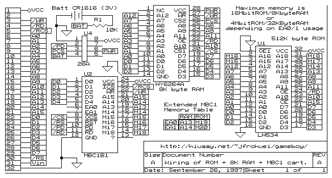
Is the first in the series of controllers which did only expand the addressable memory. Since the gameboy has 16 address pins and 8 data pins running through to the cartridge, the gameboy may without an MBC address only read from and write to a maximum of 256Kbits or 32Kbytes which is incredibly small considering Mario Land has 12 massive levels with multiple means of gameplay including the platformer and shooter, in both an airplane and submarine. Some of these levels even have secondary underworlds where Mario drops to an extra map off screen to collect secret coins or other items.

In any case, the MBC1 has two different modes to choose from. There is the 16Mbit ROM/8KByte RAM and 4Mbit ROM/32KByte RAM. 

Note: RAM is an external IC which needs to be connected to a battery while disconnected from gameboy power to retain data.

MBC2

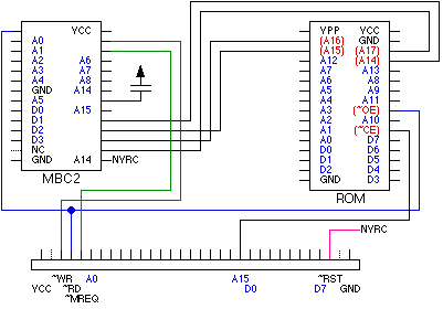
Similarly to the MBC1, the MBC2 maps extra banks of memory with specific memory writes; however, it may only map up to 2Mbits or 256Kbytes of ROM. Why a decrease? Well the magical thing about the MBC2 is that it contains 512 x 4 bits of SRAM built into the IC itself. This saves a lot of room on your cartridge board granted you are designing one.

The MBC2 can save money on RAM and space on your board if you are programming a small game that requires little ROM and RAM. Referring to the MBC1 above, if you wanted to offer a saving feature, you would need to source a RAM IC as well and route all of the Address, data and control pins to another location on the board.

MBC3

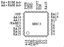
The MBC3 may again address up to 16Mbits of memory, but has a major feature built like the MBC2 has RAM. The MBC3 has an RTC or Real Time Clock built in. The RTC while still needing battery power when disconnected, offers a real-time count so that games such as pokemon may tell whether it is night or day, or when an hour in real life has passed for example.

Some games use the MBC3 without utilizing the RTC, but games that do include Pokemon of Generation 2 and Harvest Moon.

MBC5

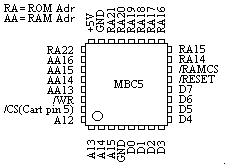
Lastly, the MBC5 is the final Memory Bank Controller from Nintendo. This particular MBC does not come with internal RAM or an RTC. It simply maps huge amounts of memory. It may map up to 64Mbits of ROM and up to 1Mbit of RAM but not both. There are different configurations to choose from; these are just the maximums.

This MBC which I find in nearly every Gameboy Color cartridge regardless of ROM size is guaranteed to work with the GBC's double speed mode. The others seem to work just fine too though, considering any GB game will run on your GBC.

For more information on how to use the MBC's with software, please refer to "Cartridge Types" in this document:
http://www.devrs.com/gb/files/gbspec.txt

MBC CPLD Clones & Reproductions

Aside from the Official Nintendo MBC's, people have had major success in recreating them using CPLD's. Both Homebrew developers and Chinese pirating companies that is.

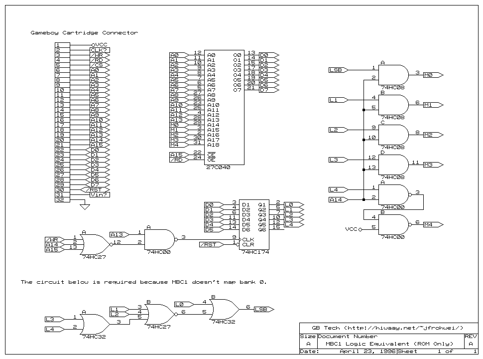
Since the MBC2 and MBC3 contain separate ICs, recreating them is much too difficult for a single person. MBC1 and MBC5 on the other hand can and have been redesigned by using CPLD's. They way they work as mentioned above is that they look for specific data bytes to be written to specific address locations. This Logic can be entirely drawn out using logic gates, which in turn can be programmed onto the CPLD.

MBC1 - CPLD

The MBC1 being the most simple, can be drawn using as little as 11 gates! (granted you do not need RAM)


MBC5 - CPLD

The MBC5 is much more complex of course, but it has also been cloned successfully by at least two separate people using two different CPLD's. One person used the XC9536 and the other person used the XC9572.

XC9536
http://chipmusic.org/forums/topic/2988/mbc5-clone-in-cpld/
and XC9572
http://home1.stofanet.dk/hvaba/gameboy/mbc5cpld/cpldcart.html

Depending on the number of inputs and outputs, more complex logic ought to be designed using PLD's or CPLD's. Not only can you save money on IC's, but space on your circuit boards. More often than not, a logic IC will take up space on your board and have a handful of unused pins and gates which is wasteful and lazy.

As always, thanks for reading! I hope I opened someone's eyes to new and old hardware.
Cheers